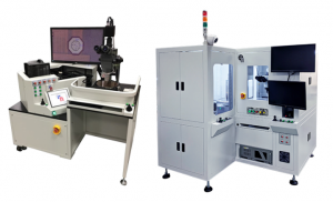
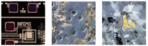
Industrial application
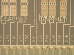
Suitable for semiconductor wafer inspection, glass panel defect inspection, probe card or IC carrier board observation
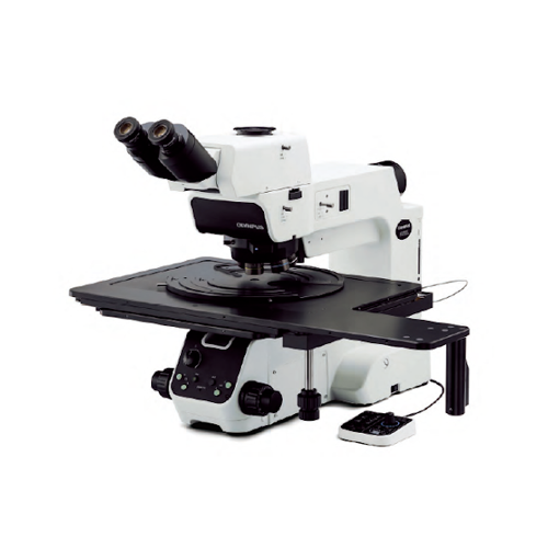
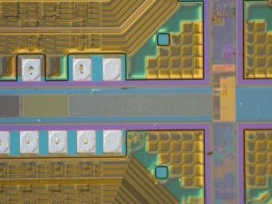
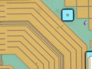
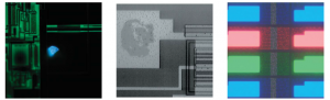
Observation method matching
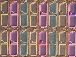
Various observation methods can be applied to the analysis of different material structures
Dark field differential interference polarized light
Fluorescent IR through light/backlight
Expanded collocation
You can also choose to use a wafer conveyor for wafer inspection.
MARCO, BACK-SIDE, MICRO observation
Fully automatic inspection of 8/6-inch wafers, fully automatic inspection of 8/12-inch wafers