Products of German Industrial Technology
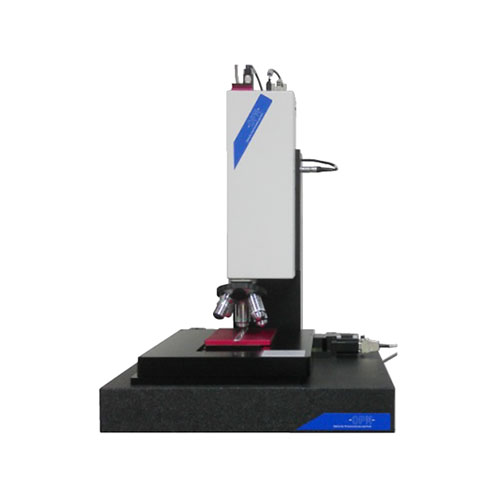
OPM white light interference + conjugate focus (two-in-one machine) originated from Germany
Features:
1. Two surface scanning modes (white light + conjugate focus)
2. 3D surface observation of microstructures for various material products
3. Z-axis 3D PROFILE measurement of small structures
4. Non-contact roughness measurement
5. Can measure the surface structure of different reflectivity and transparent materials
6. Z-axis analysis accuracy 0.01um – 0.1nm
7. It can be installed in special equipment institutions according to the size of the product.
3D scanning principle
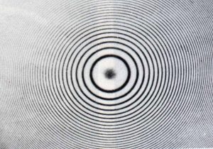
white light interferenceWhite Light Interferometry:
Pass a light source of a specific wavelength through a flat or convex mirror (DI objective lens)
Two reflections through the object produce "Newton rings" (also called interference fringes).
Its Z-axis upper and lower limit range scanning definition principle
Use the generation of interference fringes as the focal length judgment value
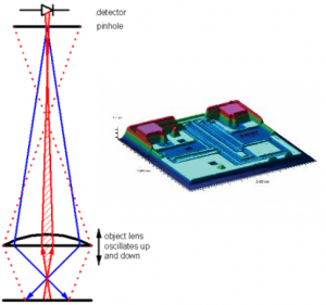
Conjugate FocusConfocal Scanning:
Pass a specific light source throughPinhole aperture excludes scattered light sources outside the focal distance
In this way, the image quality is improved by using the contrast generated by the reflected light signal.
To determine the Z-axis focal length position.
What are the advantages of two-in-one "white light interference + conjugate focus"?
Low reflectivity → conjugate focus
High reflectivity → white light interference
Transparent material → white light interference
Different material reflectivities can be used in different scanning methods to obtain more accurate results.
Depending on the lens magnification, the measurable accuracy is 0.01um – 0.1nm
Here’s why you should choose a 2-in-1 model.
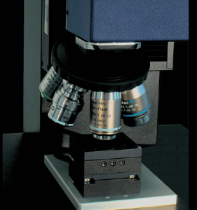
Different interference objectives and conjugate focal objectives can be installed according to needs
The objective lens nose wheel can hold up to 6 objective lenses
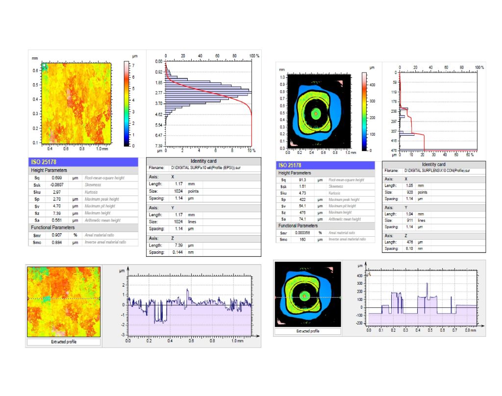
Export the scanned and synthesized report with one click;
3D image, 3D profile, automatic capture of the highest and lowest Z-axis surface structure heights, Sa surface roughness (or line roughness Ra)
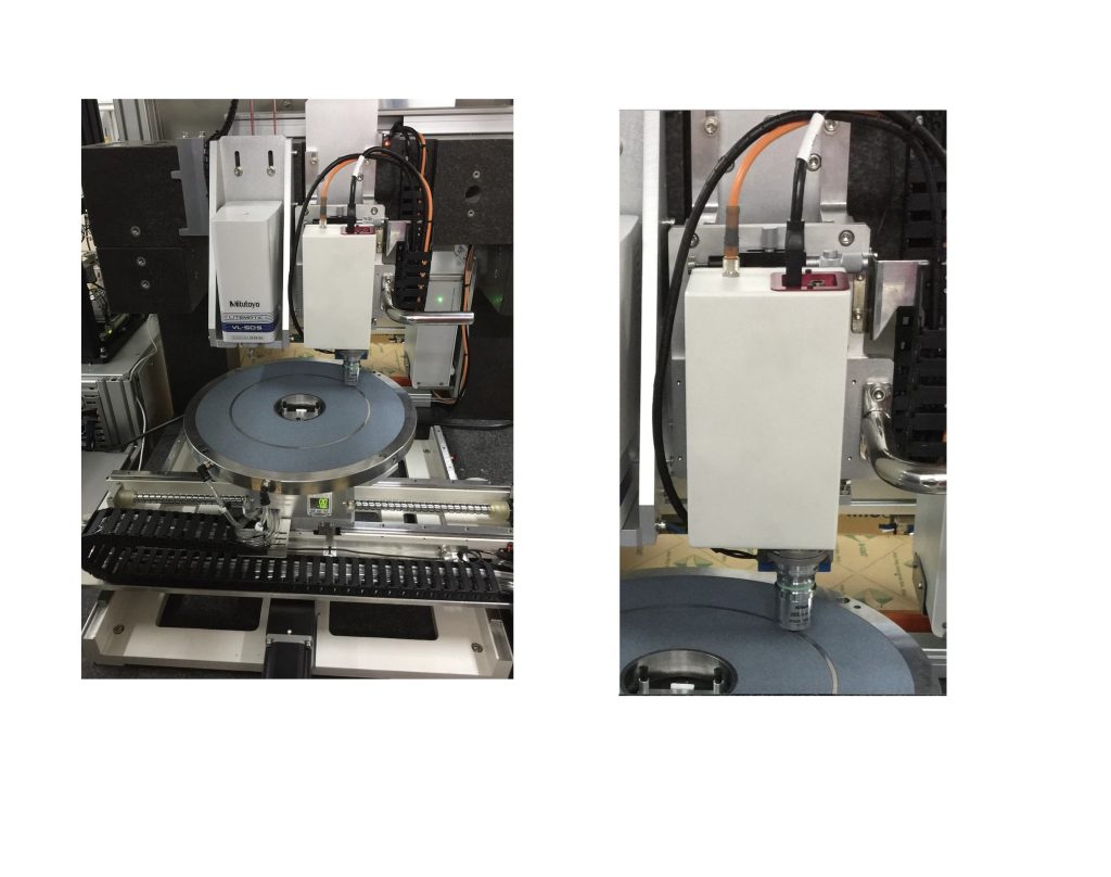
Can be integrated into various automated machines, and relevant SDKs can be opened for automation equipment integration
Practical examples
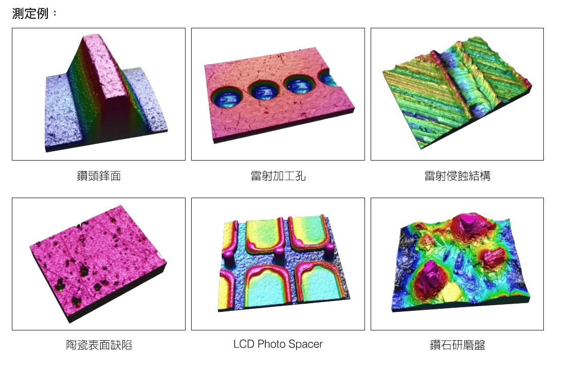
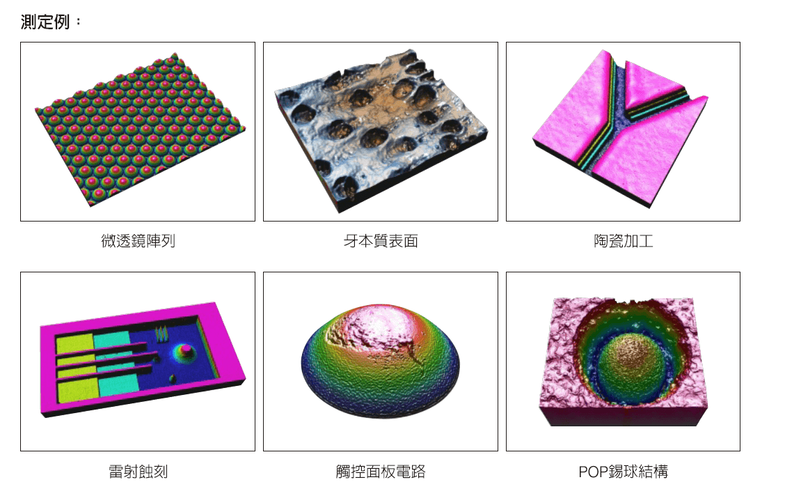
Application areas:
Bioengineering, semiconductor technology, optoelectronics technology, MEMS, optical manufacturing
Nanoengineering, steel, automobile, plastics, paper industry
Measurement items: incoming material inspection, production control, process improvement, quality inspection, fault analysis, R&D
- High-resolution 3D measurement of microstructures takes only seconds
- Can measure high and low reflection transparent materials
- Z-axis resolution can reach 1nm-0.1nm (depending on lens magnification)
- Features that can measure morphology: roughness, film thickness, height difference, 2D/3D profile, flatness, waviness, etc.